- info@moretec-inc.com
- |
- CN
- |
- JP
Sputtering is a process whereby particles are ejected from a solid target material due to bombardment of the target by energetic particles, particularly gas ions in a laboratory. It only happens when the kinetic energy of the incoming particles is much higher than conventional thermal energies. Sputtering is the thin film deposition manufacturing process at the core of today's semiconductors industry.

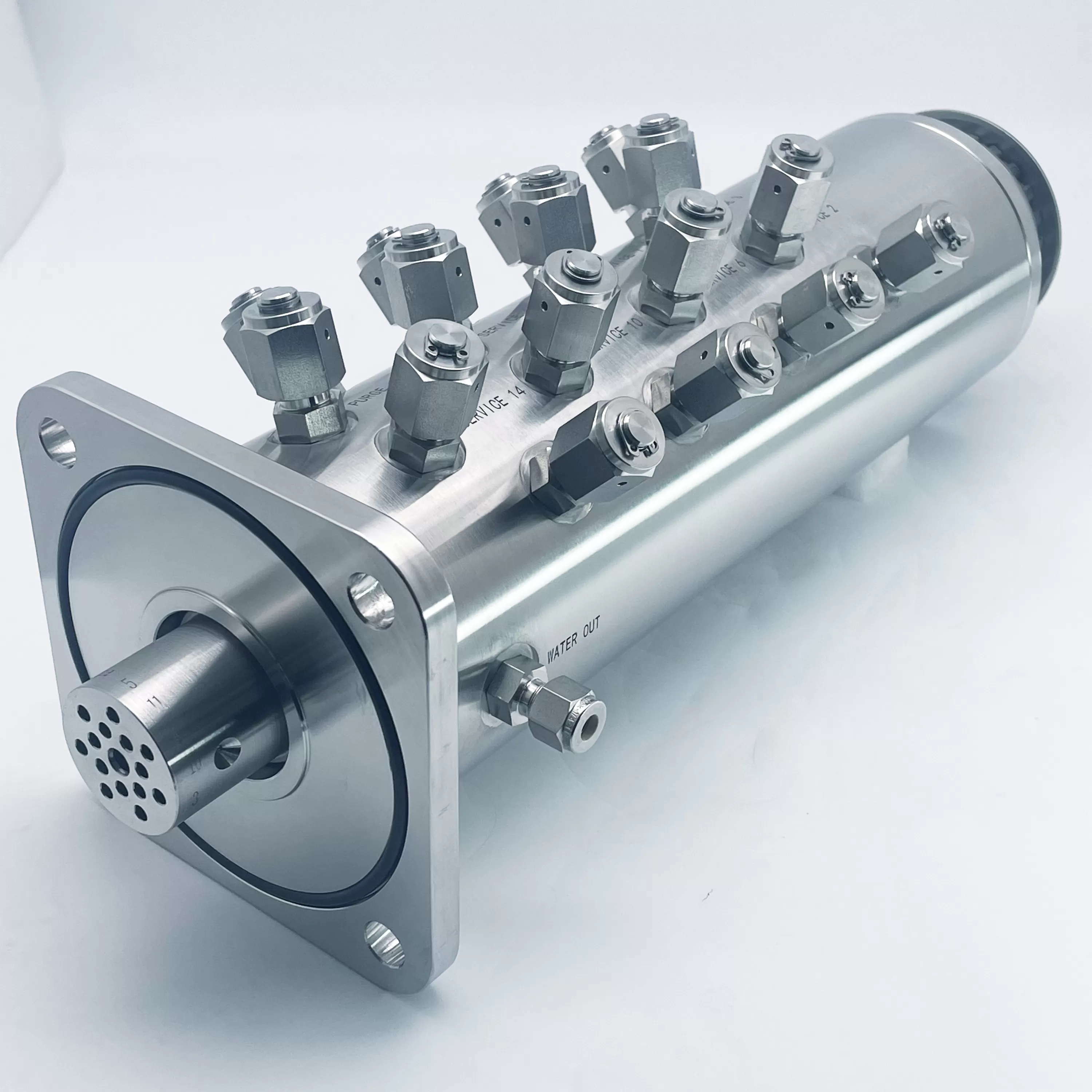
Physical vapor deposition (PVD) describes a variety of vacuum deposition methods which can be used to produce thin films and coatings. PVD coatings are formed at relatively low temperatures (400-600°C). PVD is characterized by a process in which the material goes from a condensed phase to a vapor phase and then back to a thin film condensed phase. The most common PVD processes are sputtering and evaporation. PVD is used in the manufacture of items which require thin films for mechanical, optical, chemical or electronic functions. Our ferrofluid feedthrough / ferrofluid seal / vacuum rotary feedthrough also applied to PVD Equipment. Please contact us for more details.
The CVD device is one of the thin film forming devices, which deposits a thin film of about 10 to 1000 nm on the surface of the semiconductor.
Various types of gases are used as raw materials for the thin film, but they need to cause chemical reactions for thin film formation, and the use of heat, light and plasma is utilized as the means.
It uses many advantages of chemical vapor deposition, such as rapid deposition rates, large processing areas, and uneven film formation.

Silicon wafers are produced from high-purity monocrystalline silicon ingots, which are grown using the Czochralski (CZ) crystal growth process. To ensure the highest quality standards, ingots with diameters up to 300mm are manufactured under strict quality control procedures.
Ion implantation is low-temperature process by which ions of one element are accelerated into a solid target, thereby changing the physical, chemical, or electrical properties of the target. Ion implantation is used in semiconductor device fabrication and in metal finishing, as well as in materials science research. The ions can alter the elemental composition of the target (if the ions differ in composition from the target) if they stop and remain in the target. Ion implantation cause also chemical and physical changes when the ions impinge on the target at high energy.